  Main Other useful info  Last modified 2020-06-25 |
PLL02A, AN6040, MC145109, MM48141, MN6040, SM5109 and TC9100PLL frequency synthesizer
OverviewDown-converting of the frequency to the divider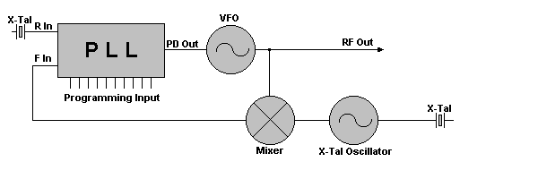 The XTAL frequency is f XTAL = f OUT - f IN
Indicated frequency steps are for a PLL02A configured for CB use. P6, P7 and P8 are normally not switched in a standard 40 channel radio, but rather fixed to either +5V or ground, depending on the design. Modification methodsA TYPICAL PLL SYNTHESIZER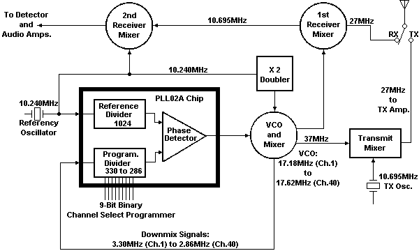 Refer to the figure, which is the PLL circuit of perhaps the most common AM PLL rig ever made. It's been sold under dozens of brand names, and uses the ever-popular PLL02A IC. The SSB and export multimode versions of this circuit are very similar; there are only minor differences relating to the SSB offsets and FMing the VCO. A PLL design may be categorized very generally by the number of crystals it uses, and by whether its VCO is running on the low or high side of 27 MHz. This particular example is actually the second generation of the PLL02A AM circuit; the original PLL circuit used a total of 3 crystals. The key to synthesizing all of the required frequencies lies in the Programmable Divider. That's the only PLL section that you can control from the outside world by means of the Channel Selector. Which is where it all starts. Suppose you choose Ch., 26.965 MHz. When setting Ch.1 the Programmable Divider (PD) receives a very specific set of instructions at all its programming pins, which are directly connected to the Channel Selector. This specific set which we have called its "N-Code", applies only to Ch.l. It's just a number by which any signal appearing at the PD input pin will be divided. Binary Programing Refer now to Programming Chart, which summarizes the important operating conditions by specific channel number. A chart like this one is normally included with the radio's service manual.Often though certain facts not directly related to the legal 40-channel operation are left out, so I`ll be filling in some missing blanks for you. Programming Chart for PLL02A
From this chart you see the N-Code for Ch.l is the number "330", with the numbers progressing down to "286" at Ch.40. This number 330 is the direct result of applying +DC voltages of about 5-10 VDC to certain PLL IC pins while grounding certain others. Thus, two possible voltage choices, and you'll recall that the PLL uses a digital or binary counting system instead of the decimal system people use. In a binary number system each successive chip programming pin or "bit" (binary digit) is worth exactly double (or half) that of the pin next to it: 1, 2, 4, 8, 16, etc. Thus each pin can be defined by its Power-of-2. We can also call them "1's bit", "2's bit", "4's bit", etc. A series of "1"s and "0"s appears in the chart for each of the 40 channels. A "1" means +DC is applied to that pin, and a "0" means that pin is grounded. The pin having the highest binary value or "significance" controls the number of possible channels that can be programmed. In this example the highest Power-of-2 is "256" at Pin 7, which is called the "Most Significant Bit"; the "Least Significant Bit" is Pin 15, which is only worth a "1" in binary. A chart like this showing the logic states of each PLL program pin for each channel is called a "Truth Chart" and is helpful for troubleshooting. How exactly was the number "330" decided? In Chart you see the truth states for Ch.l only. Above each PLL program pin are numbers I`ve labelled "P0WERS 0F 2", such as 1, 2, 4, on up to 256 which is how a binary counter counts. By adding up the weight or significance of every pin showing a "1", the N-Code is determined. The "0" or grounded pins are always ignored. In this example we have: 256 + 64 + 8 + 2 = 330. Go back now to Programming Chart and notice how the logic states for Pin 7 and Pin 8 never change at all for any of the 40 channels. Then look again at Figure 11 and you'll see that those pins are permanently hard-wired such that Pin 7 is always tied to +DC ("1"), ana Pin 8 is always grounded ("0"). You'll often find that many service manuals won't even include these pin states in the Truth Chart because they never change when programming for the legal 40 channels only. This is a case of those missing blanks I'm filling in for you, and you can test this idea by checking the rig's schematic. Compare the total programming pins available to the total number needed for 40 N-Codesl it's an obvious modification source. The original 18-channel Australian CB service was legally expanded recently to match the 40 FCC channels. Many of the older Aussie rigs, especially those with the Cybernet type PLL02A chassis, are simply American rigs with a limited Channel Selector switch. These can be easily expanded by replacing the 18-position switch and wiring up the unused binary bits on the PLL chip. For example, the original Australian Ch.1 was 27.015 HHz, which corresponds to U.S. Ch.5. The N-Code here is "325". The N-Code for their old Ch.18 (27-225 HHz) is "304". Reprogramming an old PLL02A rig for N-Codes greater than "325" or less than "304" expands the channels. This particular IC, the PLLO2A., has a total of 9 binary programming pins, pins 7-15. So it has what's called a "9-bit" binary programmer. Some quick math should tell you that the chip has a potential channel capacity of 29 - 1, or 511 channelsl (1+2+4+8+16+32+64+128+256 = 511). 0nly 40 channels are used for CB purposes but by proper connection and switching of unused pins, many more frequencies are possible. The VCO Circuit Refer back to Figure. This VCO runs in the 17 MHz range, from 17.180 MHz on Ch.1 to 17.62 MHz on Ch.40. The VCO is controlled by an error voltage received from the PD, which is constantly looking for a match at the output of the Reference Divider and Programmable Divider. The Reference Divider is accurately controlled by a 10.240 MHz crystal oscillator whose signal is divided down digitally by 1,024 to produce the required 10 kHz channel spacings. If the Programmable Divider should also happen to output the exact same 10 kHz the result would be perfect; no correction from the PD, and the loop would be locked. What would it take to produce a perfect 10 kHz output from the Programmable Divider? We've alredy seen that the Programmable Divider is set to divide any signal it sees by the number 330. For example if it should see a signal of exactly 3.30 MHz at its input, the resulting output would be 3.30 MHz + 330 = 10 kHz. So if we can somehow get an input signal of 3.30 MHz, everything will fall perfectly into place. Loop Mixing It so happens there's a very easy way to do this by cleverly borrowing a bit of existing circuitry. If some 10.240 MHz energy from the Reference Divider is taken off and passed through a tuned Doubler stage, the result would be 2 x 10.240 = 20.480 MHz. Here's where that very important loop mixing principle enters; by mixing the 20.480 MHz signal with the Ch.1 VC0 signal of 17.180 MHz, sum and difference frequencies are generated. The sum is 20.480 + 17.180 = 37.660 MHz. The difference is 20.480 - 17.180 = 3.30 MHz. Just what's needed to lock the loop. And the 37.660 MHz energy isn't wasted either; it's used as the high-side mixer injection signal that produces the first- RX IF: 37.660 - incoming 26.965 = 10.695 MHz IF. Phase Detector Correction What happens if the mixing product to the Programmable Divider isn't exactly 3.30 MHz? Let's find out. Since the N-Code is 330, a signal of other than precisely 3.30 MHz would produce a slightly different output to the PD. For example a signal of say, 3.10 MHz results in 3.10 MHz + 330 = 9.39393 KHz. The PD will sense this error and try to correct it by applying a DC voltage to the VC0. This correction voltage will drive the VCO up or down slightly in frequency, with the PD always comparing its two inputs, until an exact match occurs again. While this appears to be just a trial-and-error process, the whole thing happens in the time it takes you to change from Ch.1 to Ch.2 ! Receiver IF`s We've now seen how the Ch.1 PLL mixer signal of 37.660 MHZ provides the RX first IF injection. Now note from Figure that we can make even a third clever use of the 10.240 MHz Reference Oscillator. By mixing that with the 10.695 MHz first IF, the result will be 10.695 - 10.240 = 455 kHz, the second RX IF. (The sum product is ignored.) Pretty smart these engineers... Almost all AM or FM CBs use this method of dual-conversion for their receivers. It's also commonly used in car radios, scanners, FM stereos, etc. where a lot of the circuit hardware already existed. Transmitter Section In this example the TX carrier frequency is produced very simply. A local oscillator of 10.695 MHz is also mixed with the 37.660 MHz Ch.1 PLL output. The difference is 37.660 - 10.695 - 26.965 MHz, which is then coupled through various tuned circuits and the standard RF amplifier chain. The Truth Chart is the most important first step in determining how a modification can be made. or if it can be made. Let's examine it in greater detail now. The exemple just described was a very easy PLL circuit using the binary type of programming code. It's quite possible for the same chip to have different N-Codes depending upon how many crystals are used, or if it's AM or AM/SSB. The preceeding circuit is one of severel used with the PLL02A; this is the "2-crystal AM" loop. It used N-Codes from 330 Ch.1 to 286 Ch.40, because those were the numbers needed for exact division, correct IFs, etc. An earlier AM loop used 3 crystals and N-Codes which went up, from 224 Ch.1 to 268 Ch-40. And in the ever-popular SSB chassis the N-Codes were 255 down to 211. Notice that these N-Codes can go up or down with increasing channel numbers. It depends on the VCO design. Those Infamous Channel "Skips" Meanwhile, let's return to a portion of Programming Chart to study some of its other features. This Programming Chart is an example showing only the channel number, frequency, end N-Codes from the original full chart. Notice anything unusual in the N-Code sequence going from Ch.1 to Ch.40? The codes aren't all consecutive and skip some points that aren't legal CB frequencies. For example, Ch.3 is 26.985 MHz, and Ch.4 is 27.005 MHz. So what the heck happened to 26.995 MHz? Gee, it's not a legal FCC channel. This is known to CB`ers as an "A" channel, in this case, Ch.3A. There are also skips at Channels 7, 11, 15, and 19. And Ch.23, Ch.24, and Ch.25 of the FCC CB band are assigned out of sequence. (That's left over from the old 23-chennel days.) What this means is that all the N-Codes as well as VCO end mixer frequencies are also out of order in the chart. Meny European countries that originally allowed only 22 channels simply adopted the Americen scheme exactly for those first 22 channels. Australia had 18 channels whose numbers didn't correspond to American/EEC numbers, but many of the actual frequencies were the same. And the UK originally assigned 40 consecutive channels with no skips at all. Remember these points when studying an older model's Truth Chart, or you may think your math is wrong when it really isn't. LOOP MIXER MODIFICATIONS Now let's examine the second possible conversion method, that of changing the Loop Mixer frequency itself. This is one of the easiest ways to modify a PLL circuit having a downmix signal. A few chips like the PLL02A can be modified by either of the programming pin change or downmix change methods. The choice depends upon the total number of extra channels desired, and how much modification work you're willing to do. Changing the mixer crystal is most commonly done when jumping up to the 10-Meter HAM band. Since there's no intention of ever using the rig again for CB, it can be permanently retuned at the higher frequency. But many of you are still expanding from the CB band and adding an extra 40 or 80 channels. The European models like those from HAM International, Major, and SuperStar were basically just American model with the extra mixing crystals already there. See also the explanation of PLL pin functions |