PLL03A and PLL08A
PLL frequency synthesizer
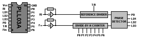
Overview
This 27 MHz band, PLL frequency synthesizer LSI chip is designed specifically for CB transceivers.
It incorporates PLL circuitry and a controller for CB applications on a single CMOS chip.
The PLL-circuit use a 7 bit ROM programmable divide-by-N counter. The ROM-table is programmed from factory to 40 channels.
| Pin | Name | Description |
|---|
| 1 | Vcc | Positive supply voltage |
| 2 | RI | Referency oscillator input |
| 3 | LD1 | Loop detected 1 |
| 4 | LD2 | Loop detected 2 |
| 5 | LD3 | Loop detected 3 |
| 6 | PD | Phase detector output |
| 7 | T/R | Transmit=High Receive=Low |
| 8 | F in | VCO frequency input |
| 9 | P6 | Programmable input 6 |
| 10 | P5 | Programmable input 5 |
| 11 | P4 | Programmable input 4 |
| 12 | P3 | Programmable input 3 |
| 13 | P2 | Programmable input 2 |
| 14 | P1 | Programmable input 1 |
| 15 | P0 | Programmable input 0 |
| 16 | GND | Ground |
Programming Chart for
PLL03A (U.S. - AM)
PLL08A (EEC - FM)
| Channel | RX
Divided by | TX
Divided by |
|---|
| 1 | 1206 | 1297 |
| 2 | 1208 | 1299 |
| .. | .... | .... |
| 22 | 1258 | 1349 |
| .. | .... | .... |
| 40 | 1294 | 1385 |
NOTES:
- Special divided-by-2 circuit in TX mode change referency divider output to 2.5kHz steps.
- 91-count upshifts on TX provides 455kHz offset for receiver IF mixing when VCO frequency is doubled.
- Since chip cannot divide VCO directly, it is down-mixed with the 10.240 MHz referency oscillator signal, producing
6 MHz outputs (RX Mode) and 3 MHz outputs (TX Mode) into dividers. Standard 16 MHz VCO is used.
- PLL08A contains only the first 22 FCC channels for EEC use, otherwise both chips are identical.
Example of VCO determination, channel 1:
1206 x 5 kHz + 10.240 MHz = 16.270 MHz (RX-Mode)
1297 x 2.5 kHz + 10.240 MHz = 13.4825 MHz (TX-Mode)
(13.4825 MHz x 2 = 26.965 MHz)
See also the explanation of PLL pin functions
|